
Intel on Intel: Foundry Renaissance, Quantum Silicon, Next-Gen Memory, Physical AI & Partnership Power Plays
The most comprehensive look at America's most valuable asset. From History to Future.

INTC 0.00%↑ Intel maintained its reign for so long that no one thought it could fail. Inevitably, it did. However, the comeback kid is here to play. In the AI arms race, Intel stands as the ultimate underdog. It is overshadowed by the likes of Nvidia and AMD, who have mastered marketing, yet quietly positioning itself as America’s semiconductor lifeline. Intel’s story is one of grit, reinvention, and strategic necessity. Let’s break it down.
Part 1: History
Intel’s origins trace back to July 18, 1968, when Gordon Moore and Robert Noyce founded the company in Santa Clara, California. Born from Fairchild Semiconductor alumni, it pioneered memory chips before dominating microprocessors with the x86 architecture. The 1971 Intel 4004, the world’s first microprocessor, ignited the PC revolution.
For decades, Intel ruled. Its “Intel Inside” campaign became synonymous with computing power. By the 1990s, it powered 80% of PCs worldwide, fueling Microsoft’s Windows empire. Under CEOs like Andy Grove, who coined “Only the Paranoid Survive,” Intel navigated antitrust scrutiny and competition from AMD, emerging stronger.
But hubris set in. Intel missed the mobile shift, ceding ground to ARM-based designs from Qualcomm and Apple. Foundry leadership slipped to TSMC and Samsung. By the 2010s, process node delays, which were stuck at 10nm while rivals hit 7nm, completely eroded its edge. Revenue peaked at $79B in 2021, but market share in data centers and AI dwindled as Nvidia’s GPUs surged.
Intel’s fall wasn’t overnight. It was a slow erosion of innovation amid complacency. Yet, its legacy as America’s chip pioneer endures, making its revival essential for national security.
Part 2: Recency Bias
Fast-forward to early 2025: Intel looked terminal. Stock plummeted below $20, layoffs hit 15,000, and every analyst whispered a sale, or bankruptcy. Despite $8.5B from the CHIPS Act in 2024 to boost U.S. manufacturing, execution faltered. Delays in fabs, mounting debt ($50B+), and fierce competition from TSMC and Nvidia painted a dire picture. The narrative completely shifted: Intel was a has-been, too big to pivot, and impossible to save.
Then came the turnaround. In March 2025, Lip-Bu Tan (LBT) took the helm, replacing ex-CEO, Pat Gelsinger. It reminds me of Tom Brady stepping in for Drew Bledsoe. The rest is history. Gelsinger’s vision was bold, but the execution lagged. LBT, a venture capital veteran from Walden International with deep semiconductor ties, has brought laser focus.
The game-winning drive unfolded.
August 2025: The Trump administration takes equity stake with CHIPS Act funding. September 2025: Nvidia invests $5B in Intel stock, signaling confidence in joint AI infrastructure. October 2025: SoftBank pledges $2B amid Q325 earnings surge. Stock rebounded and 18A ramped up. Recency bias had written Intel off, but reality has proved otherwise.
Part 3: The Underdog’s Edge
Today, Intel remains the underdog, but its growth narrative is shifting. No longer just a chipmaker eating into competitors via cost efficiencies (e.g., Lunar Lake CPUs undercutting AMD on power), it’s becoming a foundry powerhouse. That’s the pivot.
The single, most crucial business (that MUST grow and gain partnerships / customers) is IFS - Intel Foundry Services.
Intel’s foundry expansion is a core part of its IDM 2.0 strategy, launched in 2021, to regain semiconductor leadership by building a world-class foundry business. Credit must be given to Pat Gelsinger for the foresight, but he will ultimately be accredited with extremely poor execution.
It separates manufacturing (IFS) from product design, treating internal units as external customers for arm’s-length efficiency.
The goal: Compete with TSM / Samsung, secure US supply chain resilience, and target $8-10B annual savings by 2025 end. Investments exceed $100B over five years, creating 10K manufacturing and 20K construction jobs.
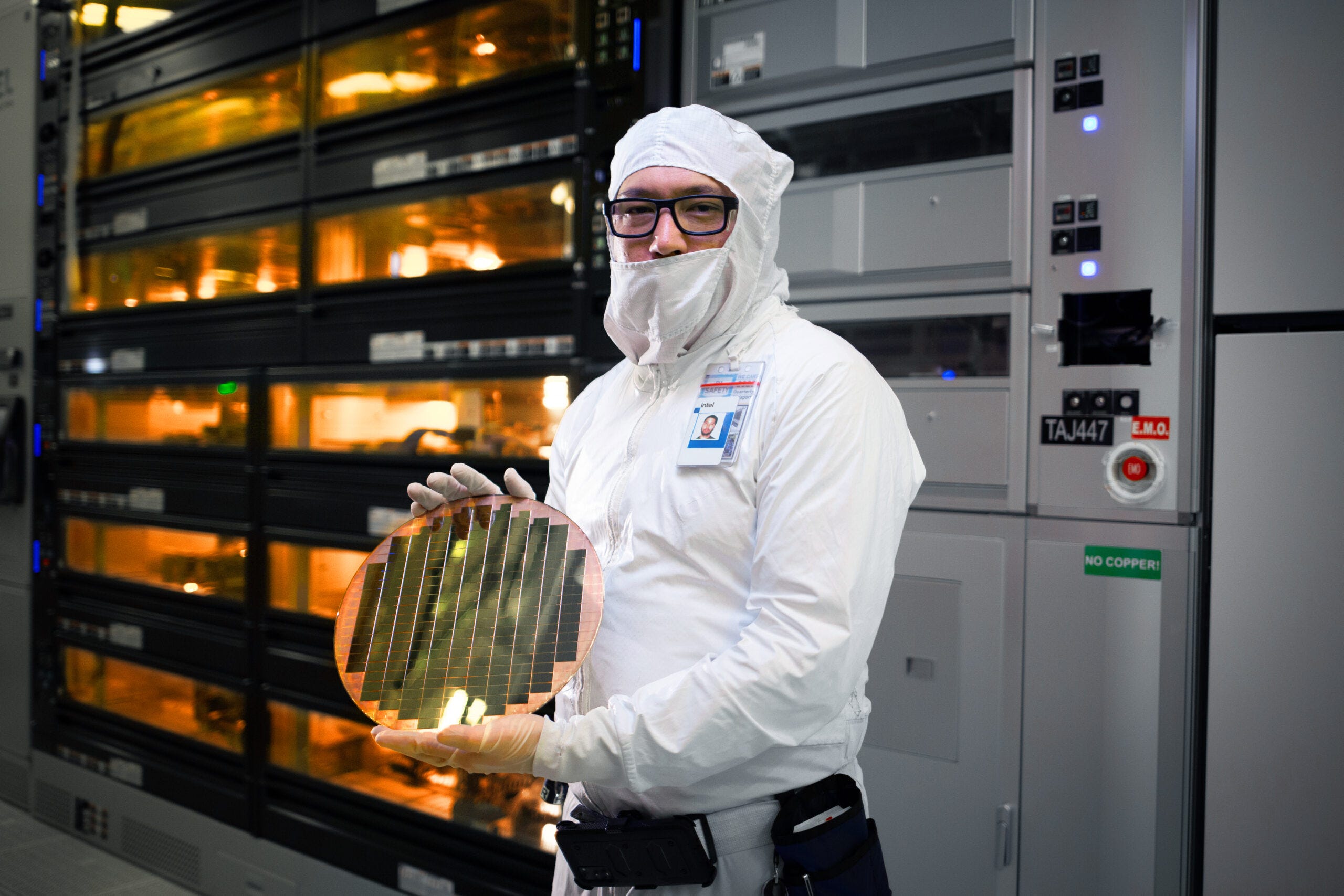
IFS is America’s greatest asset. In a world of geopolitical tensions, it hedges risks for smart players shifting from Taiwan to U.S. soil. TSMC’s Arizona fab is still tied to foreign control and vulnerabilities. Intel’s Ohio, Oregon, and Arizona expansions are domestic through and through, bolstering sovereignty in AI and beyond.
Part 4: The Roadmap Ahead
In one year, the market will no longer recognize Intel as “just a CPU company.” It will be running two AI-imperative businesses under one roof:
Intel Foundry Services (IFS): The world’s only American “pure-play foundry” at scale (with American IP and government stake).
Its own line of cost-effective AI accelerators that it can sell directly to Cisco, Google Cloud, AWS, Microsoft Azure, and the U.S. DoD. Intel will essentially have an entire TSM business, but also make AI chips that are cost-effective.
To understand the basics, let’s understand why you may hear the word “fab” referred to when speaking about TSM or Intel’s foundries. A foundry is called a fab because the actual factory that makes chips is short for “fabrication facility” (or fab for short). “Foundry” means a company manufactures chips for other companies (like a metal foundry casts parts for car makers).
For Intel, it owns both its foundry business (IFS, manufacturing for others) and its fabs (U.S.-based factories). Full vertical integration reduces Taiwan dependency, ensures supply chain control, and leverages government funding for leading-edge nodes like 18A, which is fully unique among U.S. players.
Intel is American: Unlike TSMC (90%+ of advanced nodes in Taiwan), Intel operates 15 fabs across the US, Ireland, Israel, and beyond, with ~70% of capacity stateside. Its $20B+ CHIPS Act funding accelerates domestic expansion (e.g., Ohio, Arizona sites ramping to 18A by 2026), insulating against Taiwan Strait disruptions. In a blockade scenario, Intel’s output could surge 20-30% via repurposed legacy nodes, per analyst models.
Geopolitical Tailwinds: US policy prioritizes Intel as a “national champion” is evidenced by the USG stake, and export controls favoring domestic fabs. A Taiwan crisis would trigger subsidies (potentially $50B+), boosting Intel’s market share in defense/AI chips while TSMC’s plants in America (e.g., Arizona) lag at <10% of capacity until 2028.
Diversification Momentum: Intel’s foundry pivot (IFS) are attracting partners like MediaTek and Microsoft, reducing reliance on Asian suppliers. It sources only ~20% from TSMC (vs. Nvidia’s 100%), and recent talent poaching (e.g., TSMC exec Wei-Jen Lo) accelerates tech catch-up, per Reuters. This is instant leverage for derisking supply chains.
Apple, Nvidia, AMD, Broadcom, Qualcomm, AWS, Google, and Marvell design their own chips. They then hand the blueprints to TSM in Taiwan. TSM ships the packaged chips back, and those become the M-chips in your MacBook, the MI300 in supercomputers, the Snapdragon in Android phones, etc.
Risk management is the most imperative function in any organization, and in this industry, interim mechanisms must be implemented immediately aligning to a common taxonomy:
Dual-sourcing mandates are already starting (Microsoft, Amazon, Google shifting portions to Intel 18A and / or Samsung 2nm).
US government is forcing “friend-shoring” via CHIPS act, and now equity, covenants and export controls.
Hyperscalers now model 12-24 month chip shortages in their scenario planning, driving accelerated qualification of Intel Foundry and TSMC Arizona as backstops.
Intel designs the chip, manufactures the chip, and ships the finished product itself (Core Ultra laptops, Xeon servers, Gaudi AI accelerators). No one else is involved. This is a moat.
Key Terms and what they mean:
RibbonFET: Intel’s version of Gate-All-Around transistors (GAA). Think of it as wrapping the electrical “gate” completely around the channel instead of just three sides (FinFET). This results in far less leakage, way better efficiency, higher drive current - and the chips run faster and cooler.
PowerVia: Intel flips the chip upside-down and delivers power from the back side. Frees up the front for more signal wires. 5-10% more transistors in the same area, with 4-6% higher performance at the same power.
High-NA EUV: The next-generation lithography machines (cost $400M each). They use a bigger lens to print smaller features cheaper and with fewer steps. Intel will be the first foundry in the West to ship High-NA in volume (14A node).
EMIB (Embedded Multi-die Interconnect Bridge): Intel’s clever way to glue multiple chiplets together side-by-side with tiny silicon bridges. Super-fast connection, and no giant expensive interposer like TSM’s CoWoS.
Foveros: Intel’s true 3D stacking tech. Chips are stacked on top of each other with direct copper-to-copper bonding (face-to-face or face-to-back). This gives massive bandwidth, tiny footprint, and lower power vs. traditional packaging. This is how Intel will build monster AI systems and the base dies that everyone else stacks their chiplets on.
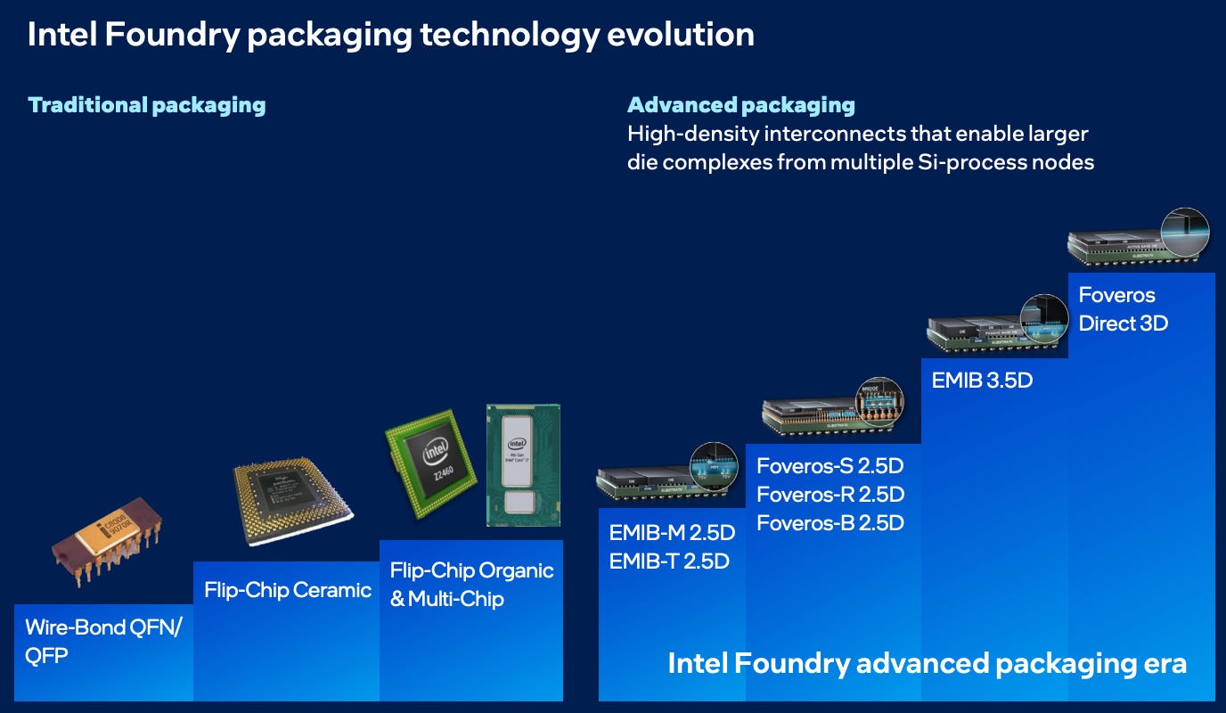
These last two (EMIB & Foveros) are the secret sauce that will enable Intel to beat TSM at advanced packaging today - and why Amazon, Google, Microsoft, and even Apple are quietly testing Intel’s lines.
In March 2021, Pat Gelsinger stood up and announced IDM 2.0, which was Intel’s ambitious plan to rebuild its process leadership while also turning itself into a serious external foundry. The idea was simple in theory and brutally hard in practice, “Make the best chips for itself while also manufacturing chips for the rest of the industry.”
Five years later, under new CEO Lip-Bu Tan, that vision is finally starting to look real. The company has become more disciplined about capital, more customer-focused, and a lot more honest about timelines. And the technology itself is now delivering.
Leading-Edge Nodes
Intel 18A family (≈1.8nm-class / angstrom-class)
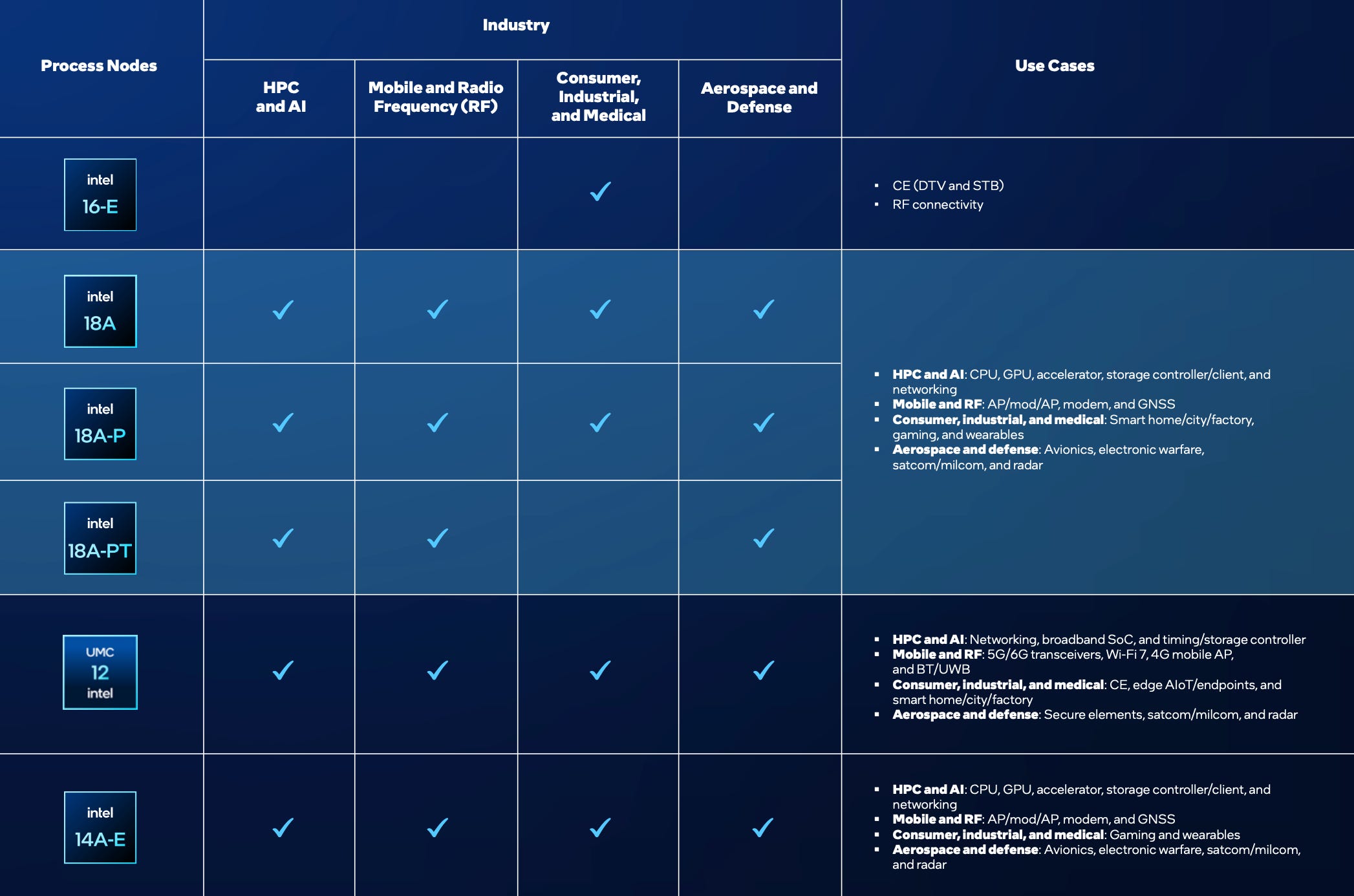
The first Western leading-edge node with RibbonFET (Gate-All-Around) with PowerVia (backside power delivery) manufactured at scale outside Taiwan / Asia.
Entered high-volume manufacturing in the US in late 2025 / early 2026.
Currently powering Intel’s own products (Core Ultra Series 3 “Panther Lake” client CPUs and Clearwater Forest Xeon).
Yields continue to improve.
Key 18A variants:
Intel 18A-P (Performance): High-performance variant optimized for compute/AI. Entered risk production (June 2026). Delivers ~9% higher performance at iso-power or ~18% lower power at iso-performance vs base 18A, plus significantly better thermal characteristics (up to 40% lower thermal resistance) and full design-rule compatibility.
Intel 18A-PT: Specialized base die with backside power delivery, purpose-built for advanced 3D stacking. Supports pass-through TSVs, die-to-die TSVs, and hybrid bonding interfaces. Targeted at large multi-die AI systems and high-bandwidth 3DIC designs.
Additional specialized variants (including low-power / mobile-optimized options and an 18A-U ultra variant mentioned in some roadmaps) for power-sensitive applications.
Intel 14A (1.4nm-class)
This is the next major node after 18A. Features second-generation RibbonFET (RibbonFET 2) and advanced PowerDirect backside power.
The official timeline under Lip-Bu Tan is risk production by late next year, into 2028, with high-volume manufacturing in 2029.
15–20% higher performance at iso-power or 25–35% lower power at iso-performance (projected gains vs 18A), with up to ~30% density improvement.
Intel 14A-E (Enhanced): Further optimized variant offering additional performance/density gains (historically cited as ~5% extra in earlier roadmaps). Targeted for 2027–2029 timeframe depending on final customer pull.
Mature / Specialty Nodes
Tower Semiconductor partnership (65nm)
A joint agreement was signed (announced in 2023) for Intel to manufacture Tower’s 65nm BCD (power management) and RF SOI technologies at Fab 11X in Rio Rancho, New Mexico.
The partnership was aimed at automotive, industrial, defense, and power management markets, but as of early 2026, Intel has largely withdrawn from this manufacturing arrangement. Tower is shifting production elsewhere (Japan). The partnership is no longer a major active growth vector.
UMC collaboration
This is a long-term partnership (announced Jan of 2024) to co-develop a 12nm FinFET process platform.
Manufactured at Intel’s Arizona fabs (Ocotillo).
Targets mobile, networking, communication infrastructure, and mixed-signal applications.
Production expected around 2027. Leverages Intel’s US capacity and UMC’s foundry expertise and customer relationships.
Discussions of deeper collaboration (including potential Super MIM capacitor tech licensing) have also surfaced.
18A Process: in detail
18A is the first true angstrom-class (roughly 1.8nm-class) process running at high volume in America. It is also the first commercial process in the world that combines Gate-All-Around transistors (RibbonFET) with backside power delivery (PowerVia).
This is the node that flips the script by providing:
First true 2nm-class chip factory running at scale in America.
Improved performance and reduced area, with PowerVia. Additionally, PowerVia has coarse pitch metals and bumps relocated to the back side of the die with PowerVia nano-TSVs in every standard cell.
PowerVia explained simply:
Intel moved the power wiring to the back of the chip. Coarse-pitch metals and bumps are now on the backside, and tiny nano-TSVs bring power up into every standard cell. This frees up the front side for better signal routing.What this actually gives you:
5-10% better density and cell utilization
Significantly lower IR drop and voltage droop
Roughly 4-6% more performance at the same power (Intel has cited up to 4% in some materials and higher in others)
RibbonFET Gate-All-Around transistors wrap the gate completely around the channel. This gives far better electrostatic control than old FinFET designs, which means better performance per watt and lower minimum operating voltage (Vmin).
Overall, PowerVia technology improves density and cell utilization by up to 5–10%, minimizes power-delivery droop, and delivers up to ~4% ISO-power performance improvement while greatly reducing IR drop compared to traditional front-side power routing.
Full support for industry-standard electronic design automation (EDA) tools and reference flows for RibbonFET and PowerVia, enabling a smooth transition from other technology nodes and allowing customers to start designing with PowerVia ahead of other back-side power solutions.
All the popular design softwares (Cadence, Synopsys, Siemens) work out of the box with Intel’s new transistors and backside power. Most competitors won’t offer that for another 2-3 years.
A robust assembly of more than 35 industry-leading ecosystem partners, providing capabilities across EDA tools, IPs, design services, cloud services, and aerospace and defense solutions, which helps ensure broad customer enablement to further ease adoption of Intel 18A.
Memory blocks, networking IP, security features, cloud design services, and defense-grade hardening), which someone else has already built and tested for 18A. It is plug and play.
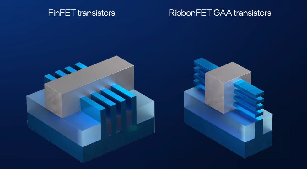
RibbonFET GAA transistors (right) offer far better electrostatics compared to FinFET transistors (left) and offer an optimized ribbon architecture for outstanding performance per watt and Vmin.
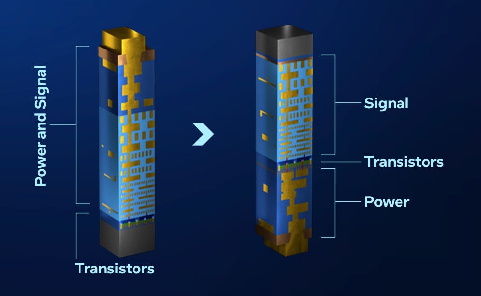
PowerVia technology enhances density and cell utilization by up to 5 to 10 percent and minimizes resistive power-delivery droop, enabling an up to 4 percent ISO-power performance improvement and greatly reducing IR drop compared to conventional front-side power routing.
14A Process: in detail
While many still think Intel is just playing catch-up, 14A is already being shown to large potential customers. Early process design kits are out, and serious engagement is underway.
This process combines the next generation of both key technologies: PowerDirect & RibbonFET 2:
Core upgrades in 14A:
PowerDirect is the 2nd-generation backside power delivery network. It is more efficient than the first-generation PowerVia, connecting power more directly to the transistors. This is a major contributor to the overall power and performance gains of the node.
RibbonFET 2 is the second-generation Gate-All-Around technology. It features tighter design rules for higher drive current, faster speeds, and better energy efficiency.
Turbo Cells are one of the more interesting new features. This is a boosted standard-cell technology that lets designers mix high-performance cells and more power-efficient cells inside the same design block. You can put the fast cells only on the critical paths (CPU max frequency and GPU critical paths) and use denser, lower-power cells everywhere else. This gives much better control over power, performance, and area for different parts of the chip.
High-NA EUV: Intel is among the first in the world to bring High Numerical Aperture Extreme Ultraviolet lithography into high-volume production. These advanced (and very expensive) tools allow finer features to be printed more cost-effectively with fewer multi-patterning steps.
Expected gains vs 18A:
15-20% higher performance at the same power
25-35% lower power at the same performance
Up to ~30% better density
14A will be the world’s top node by 2027 / 2028 with the fastest, most efficient chips being made safely outside Taiwan.
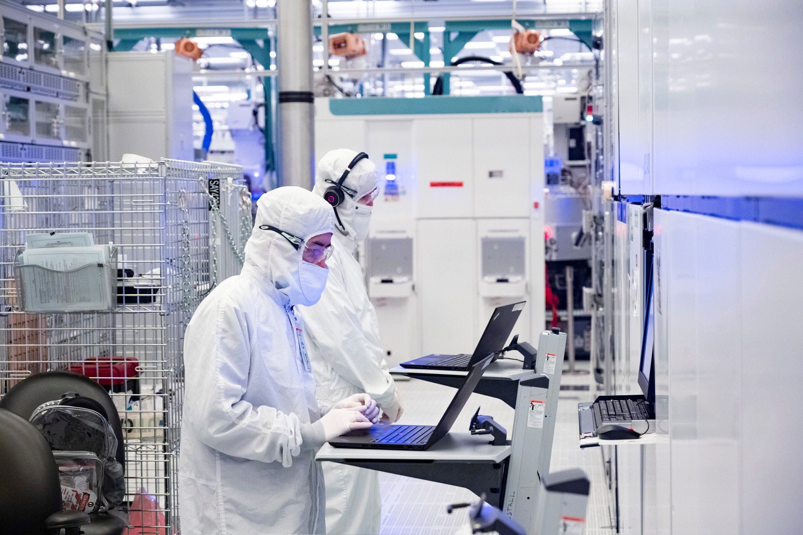
Intel isn’t just making chips for its own laptops anymore. Its foundry will crank out the most advanced silicon and packaging on the planet for every high-stakes use case:
Memory
Intel’s engagement with memory technologies has been marked by ambition and adversity. In the early decades, the company pioneered dynamic random access memory, establishing foundational contributions to the semiconductor landscape. However, escalating competition from international manufacturers prompted a strategic retreat in 1985, redirecting resources toward microprocessor dominance. Subsequent efforts, such as the collaboration with Micron on flash memory, culminated in the introduction of 3D XPoint technology under the Optane brand.
This innovation sought to merge the speed of dynamic random access memory with the persistence of NAND storage, yet it encountered substantial hurdles, including elevated production expenses and limited market penetration. By 2022, Intel discontinued Optane development, incurring significant financial impacts, and divested its NAND operations to SK Hynix in stages.
These experiences accentuated the capital-intensive nature of memory markets, characterized by price volatility and reliance on specialized suppliers. Nevertheless, Intel preserved critical intellectual assets from these endeavors, including expertise in 3D stacking and material sciences, which now inform its current strategies.
At the heart of Intel’s revival lies Next Generation DRAM Bonding, a vertically stacked architecture developed under the United States Department of Energy’s Advanced Memory Technology (AMT) program. This technology layers eight or more dynamic random access memory strata, overcoming traditional constraints to deliver superior density, bandwidth, and energy efficiency.
Prototypes demonstrated in early 2026 validate its applicability to mission-critical environments, such as national laboratories and defense systems, emphasizing reduced dependency on international supply chains. Extending this foundation, Intel’s collaboration with SoftBank’s SAIMEMORY subsidiary advances ZAM, a next-generation solution promising two to three times the capacity of high-bandwidth memory, alongside halved power consumption.
Utilizing angled interconnects for optimized spatial efficiency, ZAM targets prototypes by fiscal year 2027 and commercialization by fiscal year 2029, aligning seamlessly with the artificial intelligence expansion trajectory.
Intel Foundry Services represents a cornerstone of the company’s strategic evolution, facilitating the convergence of advanced manufacturing processes with innovative memory technologies to deliver holistic solutions for artificial intelligence and high-performance computing applications. This division merges cutting-edge process nodes, such as Intel 18A and Intel 14A, with sophisticated packaging methodologies, including Embedded Multi-Die Interconnect Bridge (EMIB) and Foveros, to enable the seamless incorporation of ZAM into custom silicon designs. Such integration yields systems that minimize latency, optimize energy consumption, and reduce overall expenditures, thereby offering a compelling alternative to traditional, multi-vendor supply chains. By bundling processors, accelerators, and memory components, Intel provides streamlined offerings that may include advantageous pricing structures, particularly appealing to operators of large-scale data centers navigating constraints in advanced packaging availability.
The Intel 18A process node, which entered high-volume manufacturing in late 2025, stands as a pivotal achievement in this framework. As of February 2026, initial yield rates range from 55% to 65%, with projections indicating progression toward 65% to 75% throughout the year. This node incorporates RibbonFET gate-all-around transistors and PowerVia backside power delivery, enhancing power efficiency and transistor density to address the demands of artificial intelligence workloads. Building upon this, the Intel 14A node is advancing toward risk production in 2027 and volume manufacturing in 2028, featuring High Numerical Aperture extreme ultraviolet lithography for further refinements in performance and scalability. Customer commitments for Intel 14A are anticipated in the latter half of 2026 and the first half of 2027, underscoring the node’s external orientation and its potential to secure substantial foundry engagements.
Packaging innovations further amplify these synergies. The EMIB technology employs silicon bridges to interconnect chiplets within a package, while Foveros enables three-dimensional stacking, allowing memory layers to be positioned directly atop logic components. In the context of ZAM, these techniques facilitate vertical DRAM stacking with angled interconnects, achieving capacities two to three times greater than high-bandwidth memory equivalents, alongside power reductions of up to 50%. This architecture mitigates traditional bottlenecks in data movement, rendering it particularly suitable for artificial intelligence training and inference tasks that require high-bandwidth, low-power memory solutions.
Strategic alliances bolster the practical application of these technologies. Collaborations with entities such as Tower Semiconductor for analog processes, Synopsys for intellectual property portfolios, and United Microelectronics Corporation for 12-nanometer nodes expand Intel Foundry Services’ ecosystem, ensuring compatibility across diverse customer requirements. Notable engagements include custom artificial intelligence silicon development with Microsoft and Amazon Web Services, as well as exploratory discussions with Apple, Nvidia, and Advanced Micro Devices for advanced node utilization commencing around 2028. Additionally, partnerships with MediaTek highlight the adoption of EMIB as a cost-effective alternative to established packaging methods, addressing supply constraints in the sector. Government support through the CHIPS Act, including equity investments, further strengthens domestic manufacturing capabilities, aligning with national priorities for supply chain resilience.
These synergies position Intel as a versatile collaborator in high-performance ecosystems, enabling the creation of integrated artificial intelligence stacks that encompass Xeon processors, Gaudi accelerators, and next-generation memory. By mitigating reliance on fragmented sourcing and leveraging US-based fabrication, Intel enhances geopolitical stability and operational efficiency, fostering a pathway toward sustained leadership in specialized segments. While commercialization timelines for integrated solutions remain subject to yield optimizations and partnership finalizations, the foundational advancements underscore substantial potential for revenue expansion in artificial intelligence and high-performance computing domains.
Google’s evolution in TPU designs exemplifies the broader industry shifts benefiting Intel. Confronted with high-bandwidth memory scarcities and Taiwan Semiconductor Manufacturing Company’s capacity limitations, Google is reportedly transitioning variants like v8e to Intel’s EMIB technology through MediaTek. This move, evidenced by MediaTek’s recruitment of specialized engineers, signals cost-effective alternatives amid supply pressures, with potential extensions to hyperscaler’s like Meta. Google’s architectures necessitate central processing units for orchestration, harmonizing with Intel’s Xeon offerings. Incorporating ZAM could solidify Intel as a primary supplier for complete artificial intelligence stacks, diversifying Google’s dependencies and accelerating Intel’s market penetration.
Robotics
Today’s robots have evolved far beyond rigid, isolated machines. They now fuse cloud intelligence, edge processing, and AI to learn continuously and adapt in real time. Exponential technological progress is unleashing entirely new abilities and applications at an unprecedented pace1.
With that, Intel is emerging as a robotics full-stack play through strategic investments, partnerships, and Xeon-powered hardware. With AI robotics, as a theme, catching steam in the markets, Intel’s bets position it for billions in the $210B market by 2030.
Intel Capital (its strategic venture capital arm) is aggressively backing humanoid robotics:
Figure AI: $9M seed in 2023, which co-led $1B Series C (Sept 2025) with Nvidia and Salesforce, valuing Figure at $39B. Funds scaling general-purpose humanoids for warehouses and homes.
RealSense Spinout: Intel carved out its AI vision arm, raising $50M for biometrics and robotics sensing.
Physical AI Strategy: Intel Vision event spotlighted robotics / Physical AI as priority, leveraging Gaudi accelerators, edge compute for affordable humanoid bots, AVs, IoT.
These stakes secure Intel’s IP in next-gen bots, blending its edge AI with startups’ agility.
Intel’s latest Xeon 6 and recently launched Panther Lake processors are built for robotics:
Humanoids: Xeon is integrated into its Robotics AI Suite2 for up to 2x faster inference for real-time decisions. Xeon also powers Figure’s prototypes. Panther Lake enables cost-effective robot controls and AI perception.
Manufacturing: Xeon W platforms (e.g., IMB-X1900 series) drive AI vision inspection and collaborative robots designed to safely work alongside humans using sensors to detect and avoid collisions in factories, cutting latency by 40%.
Autonomous Vehicles: Custom Xeon AI chips in self-driving hardware through AWS cloud - already in AGVs / AMRs for logistics.
Mobileye: Intel’s autonomous driving subsidiary (acquired in 2017 for $15.3B), extends robotics via AV tech for robotaxis and commercial bots.
Key Ties:
Robotaxi Partnerships: Mobileye Drive with VW, Rimac (Verne), Chinese OEMs for Level 4 / 5 autonomy in shuttles / vehicles, revealed during CES 2025.
Tech Integration: EyeQ6 / Ultra chips (on Intel 5nm) for vision, mapping (REM), AI in AVs / robotics, influencing edge AI for industrial bots.
Nvidia-Intel collab (via its equity stake) enhances OpenVINO for robot AI, outpacing AMD in edge compute.
AWS / Google Cloud’s Xeon exclusivity locks in Intel’s hyperscaler volume, while robotics deals add $500M+ revenue streams.
Amid the whole AI hype, Intel’s 18A process validates its turnaround, where humanoids alone could hit $38B by 2035, according to Goldman Sachs.
Quantum Computing
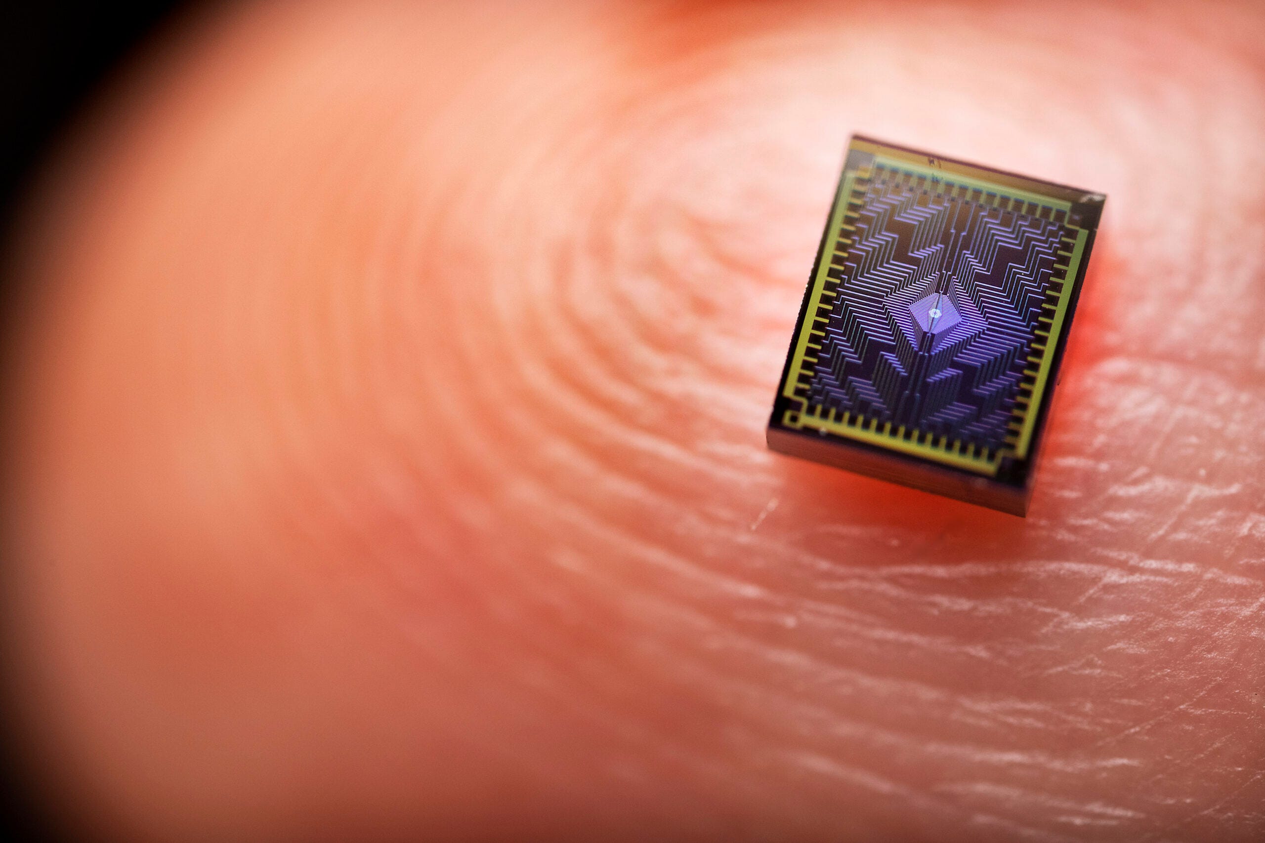
Intel’s approach to quantum computing centers on silicon spin qubits, which utilize the spin states of electrons in silicon to encode quantum information. This methodology aligns with the company’s core competencies in transistor fabrication, enabling the production of quantum devices using established 300-millimeter wafer processes.
A pivotal development is the Tunnel Falls chip, a 12-qubit silicon spin qubit device introduced in 2023 and made available to research institutions to foster ecosystem growth. Tunnel Falls achieves high fidelity, with metrics such as 99.9 percent gate fidelity in single-qubit operations, positioning it as a foundational tool for advancing quantum research.
Building on this, Intel continues to refine its quantum hardware. Recent efforts include enhancements in qubit density, uniformity, and error correction, essential for fault-tolerant systems. For instance, the company explores cryogenic control chips like Horse Ridge, which manage qubit operations at low temperatures, addressing scalability challenges in quantum systems. Future developments aim at million-qubit scales, with quantum dots serving as building blocks for dense, reproducible arrays. These initiatives reflect Intel’s commitment to bridging quantum and classical computing through hybrid architectures.
Quantum Computing Ecosystem Layers
Infrastructure: Foundational support for quantum hardware, including advanced cryogenics, vacuum systems, and shielding to preserve qubit stability.
Quantum Processing: Core layer where quantum computations occur; dominant modalities include trapped ions, neutral atoms, superconducting circuits, and photons, with silicon spin qubits emerging strongly; also encompasses networking components like interconnects and quantum memories for distributed systems.
Control and Readout: Interface managing classical-to-quantum translation, error handling, and result extraction.
Middleware: Operational software stack, including programming languages, SDKs, compilers, optimizers, and schedulers.
Applications: End-user layer with algorithms and software; currently challenging due to limited hardware power, but expected to capture significant value over time, similar to classical computing evolution.
Intel’s quantum endeavors are amplified through strategic alliances that accelerate research and industrialization. A longstanding collaboration with QuTech, the quantum institute of Delft University of Technology and TNO, dates back to a $50 million investment in 2015, focusing on scalable quantum systems. This partnership has yielded advancements in spin qubit fabrication and control.
In February, Intel signed a Memorandum of Understanding with Japan’s National Institute of Advanced Industrial Science and Technology (AIST) to develop large-scale silicon-based quantum computers, leveraging Intel’s manufacturing prowess for next-generation prototypes.
Additionally, Intel joined the Chicago Quantum Exchange, collaborating with institutions to advance quantum engineering. These efforts extend to ecosystem partners like Quantum Machines, ensuring integrated solutions from hardware to software.
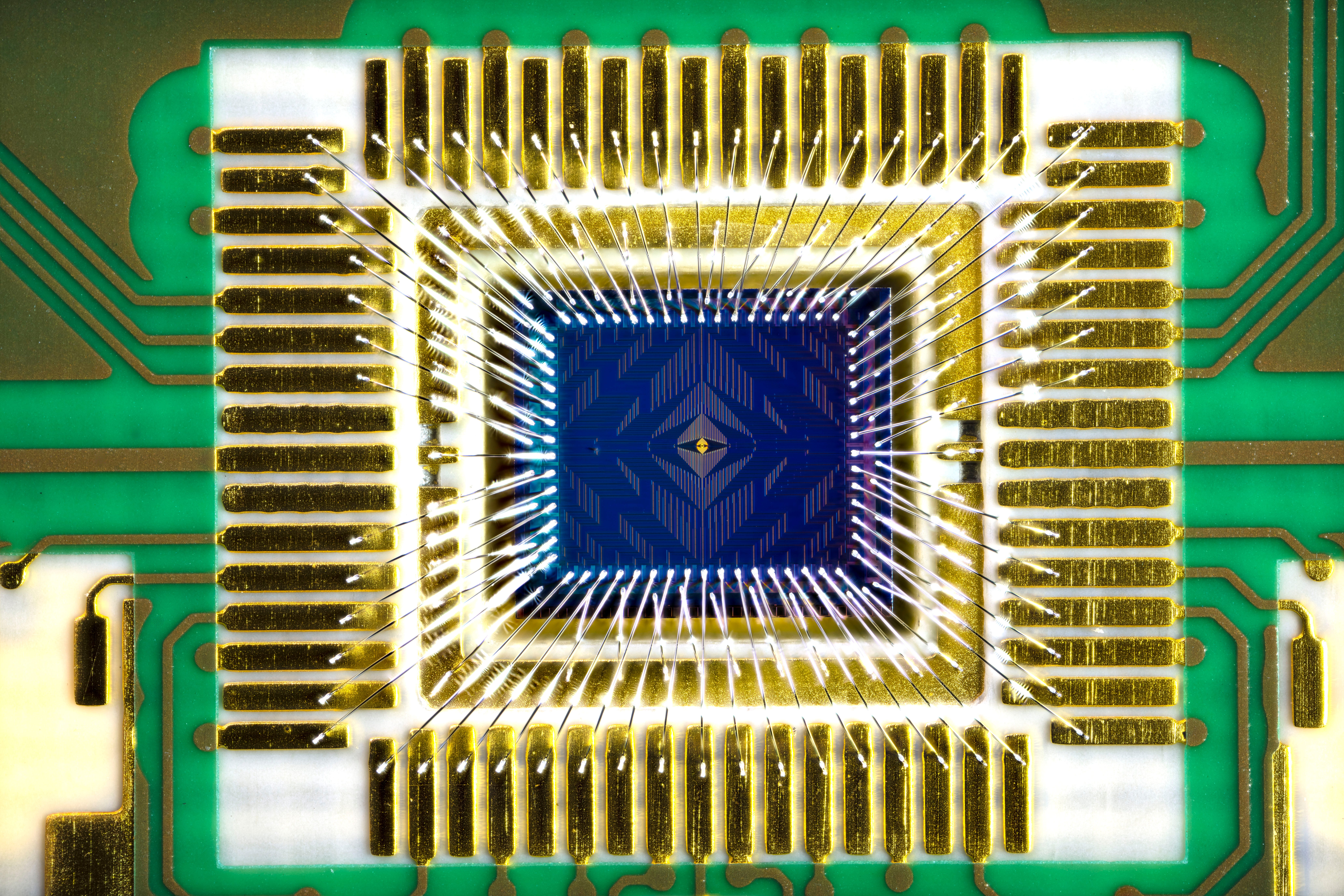
Intel Labs is working to achieve quantum practicality, the transition of quantum technology from the lab to commercial quantum systems that solve real-world problems. With the help of industry and academic partners, Intel has made significant progress in realizing this vision.
Intel is building a complete, manufacturable quantum computing stack centered on silicon spin qubits, leveraging its unmatched CMOS transistor expertise for scalability that most competitors lack. Goal: practical systems with >1 million qubits solving real problems in chemistry, materials, drug design, optimization, finance & cryptography. Here’s the comprehensive picture from Intel’s official research and key milestones.
Silicon Spin Qubits & Tunnel Falls
Intel’s core bet is silicon spin qubits in Si/SiGe quantum wells (isotopically purified for longer coherence times by reducing magnetic noise). Advantages vs superconducting qubits: much smaller devices, potential for “hot” qubits operating at higher temperatures (easier cooling/scale), and seamless integration with existing high-volume 300mm CMOS manufacturing. This enables the uniformity, yield, and cost curve needed for million-qubit systems.
Tunnel Falls, announced in June of 2023, is Intel’s most advanced silicon spin qubit chip released to researchers:
12-qubit device (linear array of 12 quantum dots). Fabricated on 300mm wafers at D1 fab using EUV lithography and advanced CMOS processes (gate/contact tech).
It achieved a ~95% yield across the wafer with voltage uniformity matching standard CMOS logic. Each wafer yields >24,000 quantum dot devices, while chips support 4–12 simultaneous qubits depending on config. Distributed via U.S. LPS Qubit Collaboratory to universities/national labs. Next-gen chip already in development (focus on quality/fidelity improvements, expected 2024+).
Argonne National Lab recently deployed this demonstrating CMOS-compatible quantum computing, and it validates high-volume manufacturing compatibility, which is a massive edge.

Cryogenic Control: Horse Ridge I & II (Solving the Wiring Bottleneck w/ QuTech)
Controlling thousands/millions of qubits from room-temperature electronics creates an impossible “interconnect/wiring bottleneck” (too many cables, heat, latency).
Horse Ridge series (developed with long-standing QuTech partner, which is a collaboration since around 2015):
Cryogenic quantum control chip placed inside the dilution refrigerator, right next to the qubits.
1st Gen was in 2020, with QuTech: First cryogenic control chip proof.
2nd-Gen Horse Ridge (debuted December 2020): Built on Intel’s 22nm FinFET Low Power technology. Integrates key control functions (microwave pulses for manipulation/readout). Dramatically reduces wiring complexity.
2021 Nature paper (Intel + QuTech): Demonstrated high-fidelity control and programmability of silicon qubits using Horse Ridge, which is a major milestone for scalable, reliable operation. This cryo-CMOS approach is foundational for scaling beyond hundreds of qubits.
Cryoprober: High-Volume Testing Engine for Commercialization
Traditional qubit testing (one device at a time in a cryostat) is too slow for process optimization at scale. Intel’s custom cryoprober (developed with Bluefors/AEM Afore) is a game-changer: fully automated cryogenic 300mm wafer prober cooling wafers to ~1.0K chuck / 1.6K electron temperature in ~2 hours.
It probes thousands of spin qubit arrays/quantum dot devices per wafer with machine vision alignment and programmable measurements (gate thresholds, mobility, noise sources, few-electron regime, etc.). Published in Nature (2024): “Probing single electrons across 300-mm spin qubit wafers.” Enables statistical wafer-scale data and rapid feedback loops for process tweaks — orders of magnitude faster than conventional methods. Directly accelerates path to reliable, high-volume quantum chip production. Intel calls it unlike any other tool and a key pillar (alongside Tunnel Falls + Horse Ridge II) for commercialization.
Intel Quantum Software Development Kit (QSDK)
Intel released QSDK v1.0 (Feb 2023; beta Sept 2022) — a full quantum computing stack in simulation that interfaces with real Intel hardware (Horse Ridge II + spin qubit chips as available).
Key features:
- Intuitive C++ programming interface (familiar to classical developers) via extended LLVM compiler toolchain with quantum extensions.
- Quantum runtime optimized for hybrid quantum-classical algorithms (QAOA, VQE, etc.) with seamless feedback loops between classical code and quantum results.
- High-performance Intel Quantum Simulator (IQS) backends (generic high-qubit or Intel hardware-specific simulation).
- Automatic mapping/scheduling of algorithms to qubits.
- Open-source Quantum Application Building Blocks repo on GitHub and Functional Language Extension for Quantum (FLEQ).
- VS Code extension for syntax support.
- Python/C++ integration for hybrid workflows.
It lowers the barrier for classical devs to experiment with quantum subroutines and prepares software for real hardware. This is not just a simulator, and it’s engineered as part of the full-stack path to commercial systems.
Major Progress & Strategic Edge
Intel has moved from isolated qubit demos to a validated full-stack approach:
- Silicon spin qubits on industrial 300mm CMOS processes with high yield/uniformity (Tunnel Falls).
- Cryogenic control integrated close to qubits
- High-volume characterization at cryo temps (cryoprober).
Mature hybrid software stack ready for devs and hardware (QSDK).
Focus is on quality (fidelity, coherence, uniformity via isotopic Si & process control) and manufacturability first, then aggressive scaling. This manufacturing moat (reusing/adapting world-class fabs) differentiates Intel from custom fab approaches by others. Still years from fault-tolerant million-qubit systems, but foundational engineering is advancing rapidly with real silicon results, published breakthroughs, and developer tools live today. Hybrid quantum-classical systems will integrate tightly with Intel’s classical AI/hardware strengths.
Intel isn’t chasing headlines with qubit counts alone. They never do chase headlines. They’re engineering a scalable, CMOS-native quantum platform from the fab up, which is control electronics, testing, software, and qubits. This positions them uniquely for when practical quantum advantage arrives. Long-term, the silicon spin qubit and full-stack strategy looks like one of the strongest plays in quantum hardware.
Part 5: The Tech Landscape Shift
AI chips already use more electricity than 61% of the world’s countries.
Training compute is exploding, and expected to grow more than 3× every year for the next decade.
Compute power is growing so fast that memory bandwidth can’t keep up.
Relying on one island in Taiwan for the world’s most advanced chips is no longer acceptable. Geographic diversity is now a national security and business survival issue.
High-performance computing and AI designs are driving the majority of new foundry revenue.
By 2028, chiplet-based designs will overtake traditional single-piece (monolithic) chips.
Tomorrow’s best chips won’t come from making a better transistor alone, they’ll come from co-designing the entire system (silicon + packaging + software) from day one. This is Intel’s bread and butter.
Part 6: Emerging Partnerships and Rumors
Big things are happening under our very eyes…
As IFS gains momentum, partnership rumors are swirling, fueled by job postings and industry leaks that point to fabless giants diversifying from TSMC. These aren’t just whispers. They’re backed by concrete clues like specialized hiring, signaling trials and prep for production on Intel’s 18A node by year-end. Intel is actively distributing 18A process design kits (PDKs) to partners, pushing for fabless diversification amid geopolitical risks.
Apple
Apple’s rumors have ignited the latest buzz. Job listings for “DRAM Packaging Engineer” mention EMIB and 2.5D tech, suggesting potential IFS collaborations. Analyst Ming-Chi Kuo predicts Intel will manufacture Apple’s lowest-end M-series chips by mid-2027, marking an ironic return to partnership five years after Apple’s Intel breakup. This could leverage Intel’s 18A-P node for entry-level M chips, providing Apple a U.S.-based hedge against TSM/Taiwan risks. Shares surged Friday on the news, highlighting IFS’s potential breakthrough.
Among hyperscalers, current and potential partnerships amplify IFS’s edge.
Google
is deepening ties: Beyond Xeon 6 adoption for Cloud AI inference (delivering 1.38x boosts and 2x+ ROI), it’s evaluating EMIB for TPU v9 and beyond to bypass TSMC’s CoWoS constraints, booked through 2026. GOOGL 0.00%↑ Google’s TPU v8e variant is planned to utilize Intel’s EMIB-T packaging technology, marking a shift from TSM CoWoS for this model. This aligns with reports of MediaTek securing orders for Google’s v7e and v8e TPUs and exploring EMIB to address CoWoS capacity constraints. Back in February, MediaTek was reported to place a major order of packaging wafers with Intel Foundry for TPU v8e.

MediaTek
is reportedly recruiting engineers experienced in Intel’s EMIB technology to support Google’s TPU production, indicating active collaboration. This is corroborated by industry analyses highlighting EMIB as a cost-effective alternative for large-scale artificial intelligence packages.
The adoption of EMIB-T for TPU v8e reflects broader industry trends where Intel’s advanced packaging gains traction amid TSMC’s supply tightness, potentially extending to other clients like META 0.00%↑ for its MTIA chips, sources confirm Intel’s EMIB has been successfully implemented in its own products, positioning it for external growth. Meta is in discussions for MTIA accelerators using EMIB.
Cisco’s ecosystem integrations with Intel (e.g., via Broadcom’s VMware expansions) signal potential foundry plays, especially in networking and AI infrastructure.
These moves, alongside Amazon’s AWS commitments, position IFS as the resilient, domestic alternative for AI scale.
Tesla / SpaceX
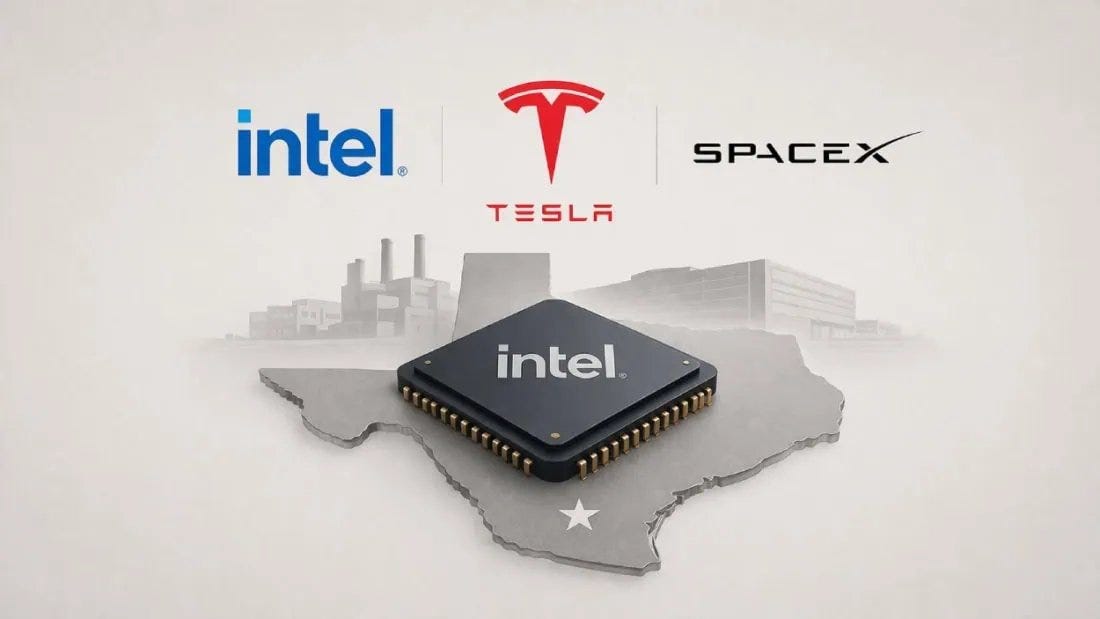
plans to use Intel 14A process node for Terafab (SpaceX + xAI +Tesla). Elon Musk is calling it the right move as the node matures. He wants memory, logic, masks, and packaging under one roof for faster chip iteration. Memory here is a very key word. Intel Foundry also may have just won a portion of AI6 manufacturing, on top of the AI7 and beyond roadmap for Terafab, originally expected to be fabricated by TSM.
Intel is now one of the future beneficiaries for Tesla’s increased capex guidance. This is now a testament to Intel’s Foundry capabilities.
First, it helps to understand what Terafab actually is. Musk announced the project in March 2026 as a massive, vertically integrated semiconductor effort centered in Austin, Texas, near Tesla’s Giga Texas. The vision is straightforward but enormous: create a single complex that handles chip design, logic fabrication, memory, advanced packaging, and testing all under one roof. The goal is to reach one terawatt of annual compute capacity. To give that number some real weight, one terawatt of compute is roughly equivalent to the output of 100 to 200 million high-end AI chips per year. That is not a modest upgrade. It is an attempt to internalize and accelerate chip production at a scale that could rival or exceed large chunks of today’s global AI infrastructure. Early stages alone call for hundreds of thousands of wafer starts per month, with plans to scale toward a million. The result would be hundreds of billions of specialized chips annually. Tesla would use the output for its AI5 and AI6 chips that power Full Self Driving, Optimus humanoid robots, and future robotaxis. SpaceX and xAI would get specialized processors, including radiation-hardened versions, for satellite constellations, potential orbital data centers, and advanced AI workloads. By keeping everything close together, the project aims to speed up iteration cycles that are normally slowed by global supply chains and distant manufacturing.
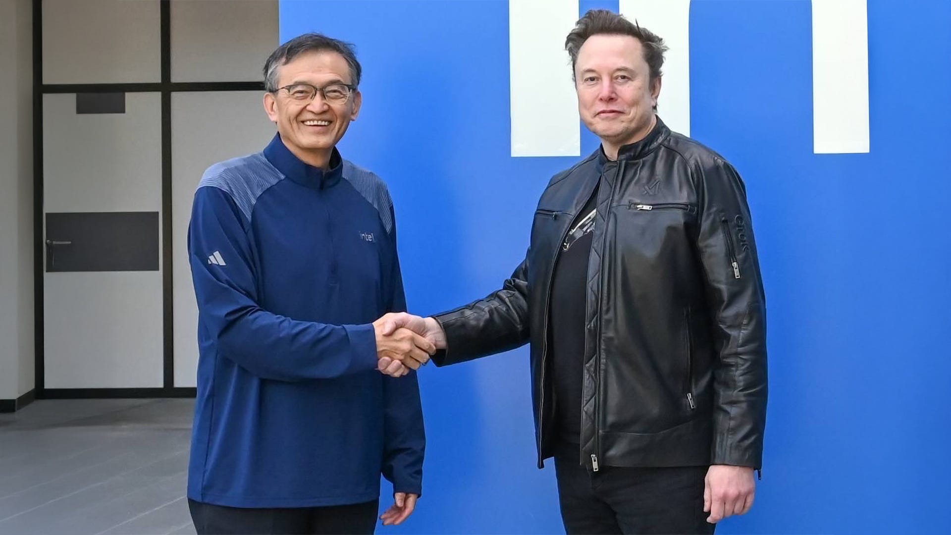
On April 7th, the company posted on X that it was proud to join the Terafab project with SpaceX, xAI, and Tesla to help refactor silicon fab technology. Intel is bringing its most advanced 14A process node, which features gate all around transistors and backside power delivery for better performance and efficiency. It is also contributing its packaging expertise, including EMIB and Foveros technologies. In practice, Intel is acting as the foundry partner, providing the manufacturing know how and scale to help Terafab hit its targets faster. This is not just another customer deal. It gives Intel the large, long term anchor demand its foundry business has been chasing.
What really changes the story for Intel is how deeply the SpaceX piece is baked in. Reports suggest a significant portion of Terafab’s output, possibly as much as 80 percent in some early planning, is targeted at SpaceX needs. These are not ordinary data center chips. They are custom, radiation-hardened designs (sometimes referred to as D3 chips) built to survive the brutal environment of orbit and beyond: intense cosmic radiation, extreme temperature swings, vacuum conditions, and tight power budgets. Terafab will produce them at scale for the next generation of Starlink satellites, for future orbital data centers that could run AI workloads in space using solar power and radiative cooling, and potentially for deeper missions tied to Starship and Mars ambitions. Intel’s 14A technology and packaging strengths are exactly what make these resilient, high-performance space-grade processors possible.
That SpaceX involvement quietly turns Intel into a space play in its own right. For years investors have viewed Intel mainly through the lens of PCs, servers, and now terrestrial AI. Through Terafab, it now has direct exposure to one of the fastest-growing frontiers in technology: the infrastructure of space itself. The satellite boom, in-space computing, and multi-planetary ambitions are creating an entirely new class of demand for advanced semiconductors. Intel is no longer just supplying chips for Earth-bound data centers and autonomous vehicles. It is helping build the silicon backbone for humanity’s expansion off-planet. That diversification strengthens the entire thesis. It gives Intel a stake in the exploding space economy while feeding hard-won lessons from radiation-hardened designs back into its own roadmap for CPUs, GPUs, and AI accelerators.
The timing lines up with Intel’s own changes under CEO Lip Bu Tan. He has been streamlining the company with cost controls, targeted reductions in headcount, and a clearer focus on making Intel Foundry Services more independent and customer oriented. Intel is moving toward a hybrid model where it still designs its own Core, Xeon, and Gaudi AI products while also serving outside clients at scale. Terafab fits perfectly here. It validates the 14A node and gives Intel a high volume partner aligned with future growth areas like AI and robotics. In a world worried about supply chain security and geopolitics, Intel stands out as the major U.S. headquartered designer with true leading edge domestic production capacity. That combination of design capability and U.S. based fabs is rare and increasingly valuable.
For Intel, the advantages run deep. The partnership secures steady work that can help improve yields and attract more customers down the line. It also pulls Intel directly into the technologies shaping the next decade: autonomous agentic AI that can pursue goals on its own, fleets of humanoid robots, and compute systems tough enough for space. Tesla needs efficient, cost effective inference silicon to scale Optimus and push toward more reliable unsupervised driving. Intel gets real world feedback from these extreme use cases that can feed back into its own roadmap. In return, Tesla and SpaceX gain a more secure and responsive supply of chips made on American soil, which could accelerate timelines and reduce risks from overseas dependencies.
The bigger picture feels significant and frankly overlooked, and not understood. AI compute demand keeps rising as models grow, robots multiply, and new applications emerge in space and autonomy. Controlling the full manufacturing stack becomes a strategic edge. Terafab’s integrated approach promises quicker innovation than the traditional fragmented model. Intel’s involvement keeps much of that progress on U.S. soil with U.S. IP, which matters for national competitiveness and security. For Tesla specifically, the collaboration could help bring down the cost and improve the performance of the silicon needed for millions of Optimus units and widespread autonomous vehicles.
This is not a guaranteed smooth ride. Building at this scale involves real challenges around capital, yields, power, and talent. Yet the foundation is there: Intel’s 18A technology is already in production, its packaging strengths are proven, and the demand signal from Musk’s ecosystem is enormous. Intel has restructured itself around its manufacturing strengths at just the right moment. By teaming up with one of the most ambitious technology efforts underway, it is moving from a company fighting to regain footing to one helping build the silicon backbone for AI, robotics, and multi planetary ambitions.
In the end, Intel’s role in Terafab feels like a narrative of quiet resurgence. The company that helped define earlier eras of computing is now embedding itself in the infrastructure for agentic AI, humanoid machines, and the compute needs of space. Chip by chip, it is helping turn ambitious visions into working hardware. The road ahead will have hurdles, but the direction is clear. Intel is positioning itself to play a meaningful part in the future of space related AI chips and the autonomous design of silicon itself. That future looks genuinely promising.
Lucky #7, Part 7: D Day
Look, Intel is working with the whole Mag 7. Don’t forget that. Intel partners with every major neocloud, and these are major collaborations. Intel is staked by the most valuable company on the planet NVDA 0.00%↑. It is staked by Softbank. It is staked by the US Government.
It is being backed by Elon Musk’s Tesla / SpaceXAI. Let us not lose sight of the fact that the most powerful people and institutions on the planet have Intel’s back. And Intel, themselves, have the superteam to execute on the backing. It is led by the most brilliant minds on the Executive team and one of the best CEOs in this space (no pun intended. the joke that never stopped).
This is America’s most valuable asset. It is the greatest company in the world, and somehow only a small % of people even understand what Intel is doing. The future of memory, the future of robotics, the future of Quantum Computing - these are all verticals that Intel has its grasps on. They have been researching and building on these areas for years. So, by the time it comes to fruition, Intel will be way ahead of everyone else. Except its investors. Only we will be there.
Intel will manufacture:
Its own CPUs / GPUs
Multiple AI accelerators (Amazon Trainium, Google TPU, Microsoft Maia, etc.)
The most advanced mobile chips outside Taiwan
All the secure chips the Pentagon needs
…all on American soil, with American IP, funded by American taxpayers, and completely vertically integrated.
A wise man once said, “the future is bright”.
Sources:
https://www.intel.com/content/www/us/en/learn/artificial-intelligence-robotics.html
https://builders.intel.com/intel-technologies/software/edge-ai-suites/robotics-ai-suite
https://www.goldmansachs.com/insights/articles/the-global-market-for-robots-could-reach-38-billion-by-2035
https://newsroom.intel.com/new-technologies/quantum-computing-chip-to-advance-research
https://www.bluequbit.io/blog/intel-quantum-computing
https://www.intelcapital.com/investing-in-the-foundation-of-quantum-computings-future-quantum-machines/
https://www.intel.la/content/www/xl/es/research/blogs/chicago-quantum-exchange.html
https://thequantuminsider.com/2025/02/07/aist-and-intel-strengthen-collaboration-for-industrialization-of-silicon-quantum-computers/
https://cen.acs.org/business/quantum-computing-chemistrys-next-AI/103/web/2025/11