
Intel: Remembering Memory
Reviving Intel’s Memory Business: Next-Gen Memory for AI and HPC.


(Image: Intel factory workers working with a High NAEU lithography tool)
The Underdog’s Return
Intel has historically navigated complex dynamics within the semiconductor memory market, marked by periods of innovation, strategic exits, and recent re-engagement through partnerships and technological advancements. This thesis examines how Intel can revitalize its memory operations and emerge as a prominent player, particularly in the context of AI and high-performance computing (HPC) demands.
Partnerships with Sandia National Laboratories and SoftBank’s SAIMEMORY subsidiary, as well as shifts in Google’s Tensor Processing Unit (TPU) ecosystem, the analysis posits that Intel’s integrated foundry model, advanced packaging technologies, and next-generation memory architectures position the company to challenge the dominance of Micron Technology, SK Hynix, and Samsung Electronics.
By offering a unified solution encompassing memory, processors, and custom ASICs, Intel can address supply chain vulnerabilities, enhance performance efficiency, and capture market share in AI-driven workloads.

Lessons from the Past
Intel’s engagement with memory technologies has been marked by ambition and adversity. In the early decades, the company pioneered dynamic random access memory, establishing foundational contributions to the semiconductor landscape. However, escalating competition from international manufacturers prompted a strategic retreat in 1985, redirecting resources toward microprocessor dominance. Subsequent efforts, such as the collaboration with Micron on flash memory, culminated in the introduction of 3D XPoint technology under the Optane brand.
This innovation sought to merge the speed of dynamic random access memory with the persistence of NAND storage, yet it encountered substantial hurdles, including elevated production expenses and limited market penetration. By 2022, Intel discontinued Optane development, incurring significant financial impacts, and divested its NAND operations to SK Hynix in stages.
These experiences accentuated the capital-intensive nature of memory markets, characterized by price volatility and reliance on specialized suppliers. Nevertheless, Intel preserved critical intellectual assets from these endeavors, including expertise in 3D stacking and material sciences, which now inform its current strategies.

The AI Memory Crunch
The rapid advancement of AI models has intensified demands on memory systems, exposing limitations in conventional technologies. Large-scale models require vast data handling, where traditional dynamic random access memory grapples with trade-offs between bandwidth and capacity, while high-bandwidth memory, integral to accelerators like Google’s TPU’s, faces supply shortages and power inefficiencies.
High-performance computing sectors, encompassing supercomputing and national security applications, necessitate low-latency solutions that prioritize energy conservation without compromising reliability. These pressures create fertile ground for alternatives that embed memory proximate to computational elements, thereby minimizing data transfer overheads and enhancing systemic efficiency. Intel’s initiatives address these precisely, targeting specialized segments where performance gains translate into competitive advantages.
Next Generation DRAM Bonding and Z-Angle Memory (ZAM)
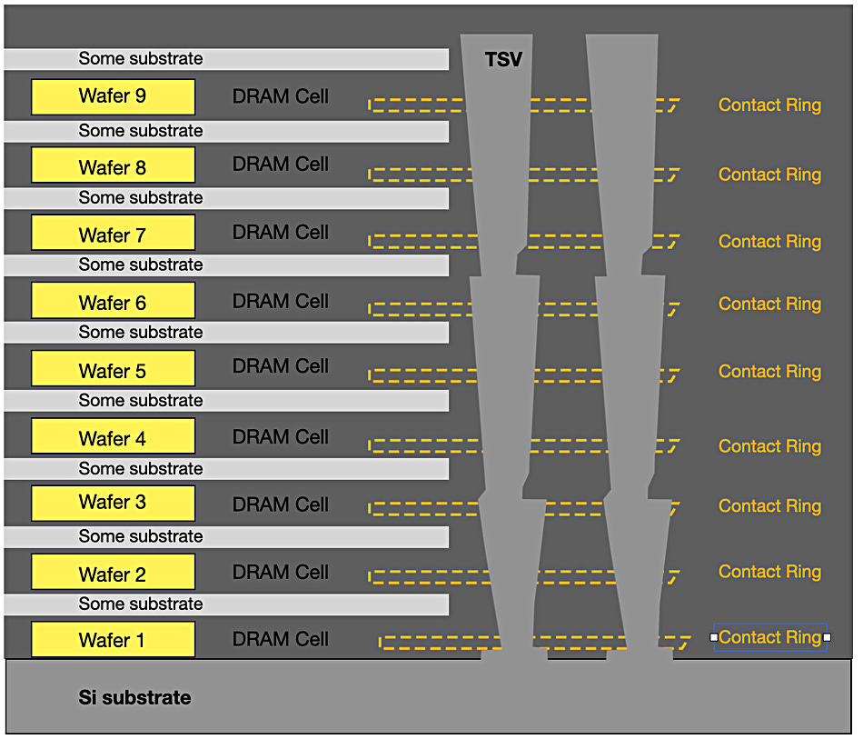
Image: Blocks & Files
At the heart of Intel’s revival lies Next Generation DRAM Bonding, a vertically stacked architecture developed under the United States Department of Energy’s Advanced Memory Technology (AMT) program. This technology layers eight or more dynamic random access memory strata, overcoming traditional constraints to deliver superior density, bandwidth, and energy efficiency.
Prototypes demonstrated in early 2026 validate its applicability to mission-critical environments, such as national laboratories and defense systems, emphasizing reduced dependency on international supply chains. Extending this foundation, Intel’s collaboration with SoftBank’s SAIMEMORY subsidiary advances ZAM, a next-generation solution promising two to three times the capacity of high-bandwidth memory, alongside halved power consumption.
Utilizing angled interconnects for optimized spatial efficiency, ZAM targets prototypes by fiscal year 2027 and commercialization by fiscal year 2029, aligning seamlessly with the artificial intelligence expansion trajectory.

Image: Getty / Bloomberg
Competitive Landscape and Revival Strategy

Against Micron, SK Hynix, and Samsung, Intel’s differentiation lies in its foundry-memory synergy, domestic American production for geopolitical resilience, and focus on specialized AI / HPC segments. While the big three dominate commodity memory, Intel can target premium, custom solutions with ZAM’s efficiency gains. Revival requires:
Scaling ZAM production through SoftBank’s investment and AMT insights.
Expanding IFS customer base for integrated AI chips.
Leveraging government contracts for initial adoption in secure applications.
Offering bundled pricing to incentivize hyperscaler shifts.
Potential risks include delayed commercialization and competition from emerging technologies, but Intel’s progress in yields (over 60% for 18A) and sold-out 2026 CPU capacity signal momentum.
Foundry Synergy: Integrating Memory with Comprehensive Solutions
Intel Foundry Services represents a cornerstone of the company’s strategic evolution, facilitating the convergence of advanced manufacturing processes with innovative memory technologies to deliver holistic solutions for artificial intelligence and high-performance computing applications. This division merges cutting-edge process nodes, such as Intel 18A and Intel 14A, with sophisticated packaging methodologies, including Embedded Multi-Die Interconnect Bridge (EMIB) and Foveros, to enable the seamless incorporation of ZAM into custom silicon designs. Such integration yields systems that minimize latency, optimize energy consumption, and reduce overall expenditures, thereby offering a compelling alternative to traditional, multi-vendor supply chains. By bundling processors, accelerators, and memory components, Intel provides streamlined offerings that may include advantageous pricing structures, particularly appealing to operators of large-scale data centers navigating constraints in advanced packaging availability.
The Intel 18A process node, which entered high-volume manufacturing in late 2025, stands as a pivotal achievement in this framework. As of February 2026, initial yield rates range from 55% to 65%, with projections indicating progression toward 65% to 75% throughout the year. This node incorporates RibbonFET gate-all-around transistors and PowerVia backside power delivery, enhancing power efficiency and transistor density to address the demands of artificial intelligence workloads. Building upon this, the Intel 14A node is advancing toward risk production in 2027 and volume manufacturing in 2028, featuring High Numerical Aperture extreme ultraviolet lithography for further refinements in performance and scalability. Customer commitments for Intel 14A are anticipated in the latter half of 2026 and the first half of 2027, underscoring the node’s external orientation and its potential to secure substantial foundry engagements.
Packaging innovations further amplify these synergies. The EMIB technology employs silicon bridges to interconnect chiplets within a package, while Foveros enables three-dimensional stacking, allowing memory layers to be positioned directly atop logic components. In the context of ZAM, these techniques facilitate vertical DRAM stacking with angled interconnects, achieving capacities two to three times greater than high-bandwidth memory equivalents, alongside power reductions of up to 50%. This architecture mitigates traditional bottlenecks in data movement, rendering it particularly suitable for artificial intelligence training and inference tasks that require high-bandwidth, low-power memory solutions.
Strategic alliances bolster the practical application of these technologies. Collaborations with entities such as Tower Semiconductor for analog processes, Synopsys for intellectual property portfolios, and United Microelectronics Corporation for 12-nanometer nodes expand Intel Foundry Services’ ecosystem, ensuring compatibility across diverse customer requirements. Notable engagements include custom artificial intelligence silicon development with Microsoft and Amazon Web Services, as well as exploratory discussions with Apple, Nvidia, and Advanced Micro Devices for advanced node utilization commencing around 2028. Additionally, partnerships with MediaTek highlight the adoption of EMIB as a cost-effective alternative to established packaging methods, addressing supply constraints in the sector. Government support through the CHIPS Act, including equity investments, further strengthens domestic manufacturing capabilities, aligning with national priorities for supply chain resilience.

(Image: Intel)
These synergies position Intel as a versatile collaborator in high-performance ecosystems, enabling the creation of integrated artificial intelligence stacks that encompass Xeon processors, Gaudi accelerators, and next-generation memory. By mitigating reliance on fragmented sourcing and leveraging US-based fabrication, Intel enhances geopolitical stability and operational efficiency, fostering a pathway toward sustained leadership in specialized segments. While commercialization timelines for integrated solutions remain subject to yield optimizations and partnership finalizations, the foundational advancements underscore substantial potential for revenue expansion in artificial intelligence and high-performance computing domains.
Google’s Pivotal Role: A Catalyst for Adoption
Google’s evolution in TPU designs exemplifies the broader industry shifts benefiting Intel. Confronted with high-bandwidth memory scarcities and Taiwan Semiconductor Manufacturing Company’s capacity limitations, Google is reportedly transitioning variants like v8e to Intel’s EMIB technology through MediaTek. This move, evidenced by MediaTek’s recruitment of specialized engineers, signals cost-effective alternatives amid supply pressures, with potential extensions to hyperscaler’s like Meta. Google’s architectures necessitate central processing units for orchestration, harmonizing with Intel’s Xeon offerings. Incorporating ZAM could solidify Intel as a primary supplier for complete artificial intelligence stacks, diversifying Google’s dependencies and accelerating Intel’s market penetration.
The Growth Horizon
This narrative illuminates Intel’s trajectory from memory retreat to prospective leadership, underpinned by innovations like ZAM and alliances that address artificial intelligence exigencies. By capitalizing on hyperscaler shifts and integrated offerings, like Google, Intel not only revives its memory operations but also fortifies its stature in the semiconductor domain. This understated evolution harbors substantial growth prospects, reshaping dependencies and fostering a robust, domestically anchored technology landscape.